Tiny-Vedas: RISC-V Infrastructure for AI Accelerator Design
Marco Spaziani Brunella, Siliscale
Download PDF GitHub (arxiv-v0)
Key results
- YOLOv3-Tiny runs end-to-end on the Alveo U280 FPGA with accuracy identical to the host (mAP@0.5 0.274089).
- One frame takes ≈296 s.
- Placed and routed on the ASAP7 7 nm process, the design reaches 540.23 MHz.
- In that layout the processor core is 3,187 µm², the vector unit is 28,466 µm², and the 8×8 matrix engine is 19,992 µm². The remaining logic is 1,874 µm².
Abstract
ASIC-based Artificial Intelligence (AI) accelerators have drawn intense interest and funding in recent years, yet their reduction to practice remained elusive. I argue that the issue relies in an old, abstraction-based development model tied to general-purpose computing CPU design.
This paper presents Tiny-Vedas, an open-source toolkit for designing RISC-V accelerators for AI, including both hardware and software for out-of-the box support for PyTorch models acceleration. At the center of the system is an in-order, single-issue, four-stage 32-bit RISC-V core supporting RV32IM integer extension and Zve32x vector extension. The core can be complemented with memory-mapped datapath accelerators to form a System-on-Chip, such as an 8×8 integer General Matrix Multiply engine.
A just-in-time compiler ingests a PyTorch model, extracts its computational graph, and turns that graph into C code that the stock RISC-V GNU Compiler Collection can build. The compiler extends cleanly to new datapath accelerators and to the pre- and post-processing they may need, such as tensor tiling.
I prove the stack with YOLOv3-Tiny vision model running on Tiny-Vedas. The design is implemented through the OpenROAD ASIC flow on ASAP7 Process Design Kit (PDK), and exercised on an AMD/Xilinx Alveo U280 FPGA.
Introduction
The recent wave of Generative Artificial Intelligence (Gen-AI) models has pushed large model operators toward designing custom accelerator silicon [1], [2] in search of better performance per watt, a broader supplier base, and lower capital and operating cost. That same demand has also drawn a crowded field of startups and open-source efforts trying to fill the gaps at different levels of the stack. Having worked inside several of them, I find the landscape sorts into three camps:
Pure-technology efforts that invent a new way to do a hard kernel—an analog General Matrix Multiply (GEMM) or an in-memory compute fabric.
RISC-V intellectual-property (IP) efforts that build high-end cores aimed at the datacenter. That market is still dominated by x86—about 87% of datacenter server CPUs in early 2025 [3]—with Arm a distant second; a large share of the spend on this kind of effort goes to bringing those cores up to run Linux, which is the wrong bar for bare-metal Artificial Intelligence (AI) acceleration anyway.
AI compiler efforts that promise a holistic software stack, pushing yet another level of abstraction on hardware that is not yet shipping. Gemmini [4] generates arrays; LLVM [5], MLIR [6], and kin lower graphs onto backends someone else already built, with bloated and rapidly-changing codebases.
In general-purpose computing, the hardware-software1 contract has always been an Instruction Set Architecture (ISA) and an Application Binary Interface (ABI), defining what operations the CPU supports, general-purpose and purpose-specific registers, and how those registers should be used by a compiler, and how memory accesses are treated. The silent, underlying assumption was the homogeneity of the systems: every general-purpose computer built in the last 40+ years had the same architectural shape. A CPU talking to a DRAM controller, with multiple level of caches interposed in between. The functionality of the system could be extended by adding a card on an expansion slot, such as a Peripheral Component Interconnect Express (PCIe) network card or a Graphics Processing Unit (GPU). The card, which we can think of as an accelerator per se, was its own microsystem that lived in a vacuum, interfacing with the main system by means of interrupts, PCIe transactions and kernel drivers.
This approach has served us well for the last five decades in computer organization and design, but it is now shortchanging us when we try to design a simple, and yet elusive accelerator system. The heterogeneous nature of these systems makes it virtually impossible to have a clean, abstracted interface between hardware and software. The same way Linux had to introduce Device Tree (DT) files to support the growing pool of heterogeneous, ARM-based Systems-on-Chip (SoCs), we need to rethink the shape of the hardware–software interface in the era of AI accelerators.
That is why I built Tiny-Vedas: an open-source, RISC-V-based AI accelerator infrastructure, composed of:
an extensible just-in-time (JIT) AI compiler (PyVedas);
a runtime eXtensible C Library (XCL).
a RISC-V core supporting RV32IM and the RISC-V Vector embedded integer profile (Zve32x);
an eXtensible Datapath Accelerator Interconnect (XDAI);
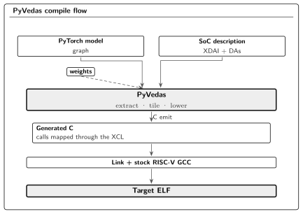
The compiler, the runtime, the core, and that bus are the stack.
Concept and Overview
PyVedas ingests a PyTorch model and a description of the target hardware, including any Datapath Accelerator (DA) present on the XDAI. It extracts the model’s computational graph and its weights, then lowers that graph into a C file whose calls target the XCL. The XCL holds the mappings from PyTorch primitives to their implementations.2 Those lowering passes extend to new DAs on the XDAI, including the pre- and post-processing they need, such as tensor tiling and quantization calibration. The C is then linked against the XCL and built with the stock RISC-V GNU toolchain.
To support a new PyTorch operator, PyVedas needs a lowering candidate and the XCL needs the matching C function—an ops.yaml row, a codegen handler, and the sources it names. To hang a new datapath, the same recipe plus the hardware YAML so the XDAI decode and the C macros share one address window. The XCL body then programs that window instead of unrolling the work into RISC-V.
Each DA is a Memory-Mapped Input/Output (MMIO) device onto the core address space. The reason why I choose to adopt an MMIO approach rather than implement custom RISC-V instruction is mainly ease of integration, and to define a clear boundary between Tiny-Vedas and third-party DAs. Supporting custom instructions means maintaining a custom version of the RISC-V GNU Compiler Collection (GCC), or an out-of-tree version of the RISC-V LLVM backend, which is simply impractical for most small teams.
As a running example throughout the paper, I choose an int8 quantized version of YOLOv3-Tiny [7], a popular computer vision model. The model is small enough to fit inside the available Static Random-Access Memory (SRAM) on the Xilinx Alveo U280 Field-Programmable Gate Array (FPGA), but complex enough to present challenges when implementing both software and hardware.
As a DA, I designed an int8 GEMM unit, representative of any third-party datapath accelerator you might want to attach to Tiny-Vedas, and used it to offload the backbone of YOLOv3-Tiny.
Compiler and Runtime Library
PyVedas starts from a torch.export graph of a PyTorch model. Each node of the graph represents an operator, like a 2D convolution or a ReLU. While walking the graph, PyVedas checks whether that operator is a lowering candidate, and when it is, looks up the matching entry in an operation dictionary, containing the mapping between PyTorch/ATEN operators and their custom C implementation in XCL.
That entry names a codegen handler and an XCL symbol (plus the C sources that implement it). The handler emits a call into the generated C file, plus any pre- and post-processing needed. After the codegen phase, the compiler hands it off to the RISC-V GNU toolchain, for final linking against XCL and ELF generation.
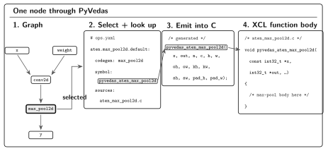
aten.max_pool2d.default from a small exported graph, looks up the XCL candidate in ops.yaml, and emits the call that the stock toolchain will compile.Figure 2 shows what a graph walk looks like: conv2d then max_pool2d. The highlighted pool node resolves to an XCL symbol in aten_max_pool2d.c. Convolution follows the same path, except its XCL body can call a DA on the XDAI (the GEMM in this paper) instead of letting GCC unroll the operator to plain RISC-V instructions. A better XCL body—or one that calls an available DA—is the same lookup; PyVedas still has to emit the call.
PyVedas extracts weights from the graph by looking for get_attr nodes and materializes them into the compile image (static buffers or the on-chip memory), so the generated Executable and Linkable Format (ELF) carries both code and parameters.3
Hardware Architecture
RISC-V Core
The core is an in-order, single-issue, four-stage pipeline, divided into a shared frontend and a scalar and vector backends. The frontend stages are Instruction Fetch Unit (IFU), Decode 0 (IDU0), Decode 1 (IDU1), while the backends are the scalar and vector Execute (EXU) as depicted in Figure 3.
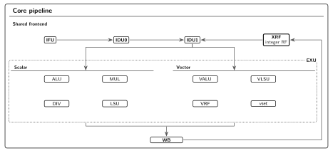
IFU maintains a program counter into the Instruction Closely Coupled Memory (ICCM). IDU0 runs the RV32IM and Zve32x decoders in parallel on the same instruction and dispatches to either the scalar or vector backend. IDU1 reads the integer scalar register file (XRF), checks the scoreboard, and issues to EXU, or stalls the frontend of the machine.
The scalar datapath is composed by an integer Arithmetic-Logic Unit (ALU), a multiply unit, a divide unit, and the scalar load/store unit (LSU). The LSU is the bridge between the core and the XDAI, connecting it to the available DAs and the memory subsystem.
The vector datapath implements Zve32x specifications, with 512-bit vectors (VLEN), 32-bit elements and unit-stride loads and stores. To keep area utilization low, the vector ALU and memory datapath are only 128 bits wide (DLEN) rather than a full 512-bit slice, so a vector op walks the register in four beats.
eXtensible Datapath Accelerator Interconnect
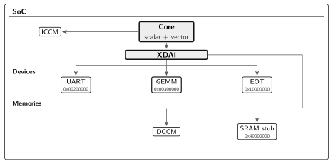
The XDAI is the Advanced eXtensible Interface (AXI) fabric the LSU uses to reach memories, peripherals, and MMIO DAs. A software-defined range decoder matches each address against the device map and steers the memory request to the target device.
This unified bus allows a DA to expose its Control and Status Registers (CSRs) to the RISC-V core. Once triggered by the core, a DA can take control of the XDAI and access any memory-mapped device, such as Data Closely Coupled Memory (DCCM) and other SRAM resources, where weights might be stored, for example, through a Direct Memory Access (DMA) engine.
The DA gives control back to the core by setting the Done CSR.
The memory map is software-defined. A device-tree-style YAML file lists each DA’s address window. Hardware uses it to build the SoC decode; the same file emits the C macros the XCL includes when it programs a DA.
Datapath Accelerators
DAs are memory-mapped, domain-specific hardware blocks used by the core to offload a particular functionality to specialized hardware. In this paper, the only DA on the XDAI is an int8 integer General Matrix Multiply (GEMM) engine, performing .
The array is output-stationary PEs with . Software writes the three bases—including —and , , , then toggles the START CSR.
GEMM’s DMA reads and from DCCM and writes to the base the core programmed, then sets the Done CSR. Figure 4 is the SoC: the core, the XDAI with that GEMM, and the ordinary peripherals—Universal Asynchronous Receiver–Transmitter (UART), end-of-test (EOT), and the on-chip memories.
Plugging the accelerator into PyVedas
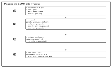
Once the DA is on the XDAI, PyVedas still has to see it: an ops.yaml row, a codegen handler, an XCL body, and the hardware YAML for the address window.
The first step is to write a codegen handler for the accelerator. That handler is the compiler’s picture of the CSR map: a base pointer for , one for , one for , the three shapes , , and , and a START bit. Those registers live in the GEMM’s window on the software-defined memory map, so that the core’s LSU can directly access those registers.
The next step is to review the primitives inside XCL and ask a simple question: which primitives could actually benefit from this DA? Matrix multiply is the obvious one. Convolution is the useful one, because a convolution is a matrix multiply after an im2col. Those XCL bodies used to be native C loops, translated into RISC-V code by GCC. To offload matrix multiplication to GEMM, I just substitute the inner multiply loop of the convolution with a call that programs the GEMM and lets its DMA engine walk and .
The last step is compile-time tiling. The engine is with . PyVedas cuts a large multiply when the packed / panels would not fit on-chip; the generated C walks those tiles, one START at a time. Figure 5 is that whole path for this GEMM.
Running YOLOv3-Tiny
To demonstrate Tiny-Vedas capabilities, I elected to run an int8 quantized version of YOLOv3-Tiny [7]: a Darknet detector with a small convolutional backbone, max-pool downsampling, a leaky ReLU after each fused convolution, an upsample/concat skip, and two linear detect heads. The Alveo U280 runs in this paper use a letterboxed input (Tiny-208). The backbone of the network is offloaded to Tiny-Vedas, while the host finishes Non-Maximum Suppression (NMS) and box decode.
Quantization and calibration
The exported PyTorch model is an integer graph: activations travel as int32, weights are int8 values held in int32 containers, and each convolution is im2col plus a GEMM DA call.
The GEMM accumulates in int32. The next layer’s pack needs those values in the int8 range. A scalar requant_i32 does that: Figure 6 is one repeating stem stage.

im2col+GEMM, leaky ReLU, requant_i32, max-pool. Detect heads drop the leaky and the pool.The pair is per layer: each layer has its own dynamic range.
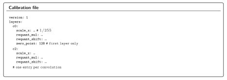
Calibration chooses those pairs offline. An FP32 run of the same net measures per-layer activation scales; I pick so , and I rewrite the bias into accumulator units. That maps most layers onto ; the detect heads keep and stay in logit units. The formula uses one for the whole layer. Per-channel weight scales are the obvious alternative: each output channel keeps its own range. Then would differ by channel, and requant_i32 would need a per channel. I left the operator scalar—one multiply and one shift for the map—so the weights share one scale. A per-channel requant would mean a vector of pairs in the operator, the calibration file, and codegen; I did not grow the kernel.
The pairs go into a calibration file that PyVedas loads (Figure 7). Since calibration is ubiquitous on quantized models, I added native calibration support to PyVedas through calibration files.
Data tiling
A Tiny-208 layer’s activations and im2col buffers do not always fit in DCCM. The JIT therefore cuts spatial and output-channel tiles so the live working set stays on chip, and moves whatever still does not fit through the 16 mebibyte (MiB) SRAM stub at 0x40000000. After a few iterations I landed on cache_col. It writes one im2col panel per spatial tile into DCCM, then walks output channels: pack a weight tile once, and reuse every cached panel. On Tiny-208 c12 that is six im2col buffers and 256 packs.
The SRAM stub is a placeholder: the same window can later be a shared level-2 (L2) cache from several Tiny-Vedas cores into High Bandwidth Memory (HBM), the way a GPU SoC is built.
GEMM tiling
Separately, every Tiny-208 convolution lowers to a matrix multiply whose , , and are far larger than with —early layers have tens of thousands of output pixels; deep layers have in the thousands. PyVedas cuts that multiply into tiles that fit one hardware job, and emits nested loops: each iteration packs a slice, rings START, and writes its piece of .
Division of labor inside the binary is simple. Convolution hits the GEMM over MMIO. Leaky ReLU and max-pool stay on Zve32x (vsetvli e32/m1, vle32/vse32, vmax/vmin).
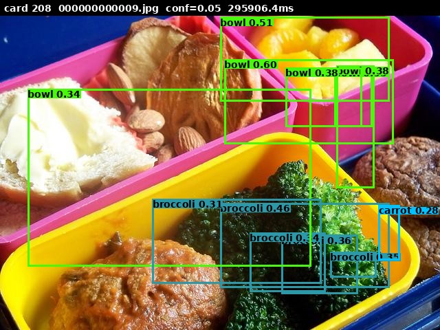
Figure 8 is the closed loop: letterbox on the host, backbone on the card, boxes back on the host. The numbers that prove it closed are in §7.
Application-Specific Integrated Circuit (ASIC) Implementation
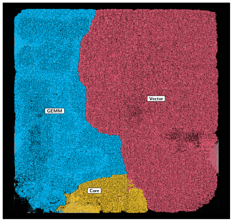
I ran the SoC—scalar core, Zve32x, and the GEMM—through OpenROAD [8] on the ASAP7 7 nm predictive Process Design Kit (PDK) [9]. Memories are ports, so Table 1 is logic only. Figure 9 is that finish. Post-route is 540.23 MHz.
| Block | Area (m) | Cells |
|---|---|---|
| Core | 3,187 | 27,000 |
| Vector | 28,466 | 258,854 |
| GEMM | 19,992 | 165,998 |
| Other | 1,874 | 14,729 |
FPGA Evaluation
The Alveo U280 sits on PCIe behind a Xilinx Queue DMA (QDMA) endpoint. The host maps a control base-address register (BAR) into the SoC. While the core is halted I write instruction memory, on-chip data memory, and the SRAM stub through that BAR; then I release the core and poll an end-of-test register. The stub is the device memory—16 MiB of on-chip SRAM today, the same window a later HBM hierarchy can occupy.
That is the split a PCIe accelerator uses. The host letterboxes the frame, builds the integer canvas, and loads the ELF, the weights, and that canvas. The card runs the backbone: convolution on the GEMM, leaky ReLU and max-pool on Zve32x. When end-of-test fires, the host reads the detect heads back over the same BAR, decodes boxes, and runs NMS.
To verify accuracy I used Tiny-208, coco128 with sixteen images, integer weights, and --cal with the requant calibration file of §5. On the host, int32 mean Average Precision at Intersection-over-Union 0.5 (mAP@0.5) is 0.274089. On the card, the same graph is 0.274089 at 80 MHz. Separately, one Tiny-208 frame with cache_col finishes in 295907.7 ms (Figure 8).
Related Work
TVM, MLIR, and IREE compile a graph onto a backend that is already there [6], [10], [11]. I needed the other direction: a new MMIO engine on a RISC-V SoC, named from PyTorch, still built by stock GCC.
Gemmini generates a systolic array and evaluates it on FireSim [4]. I start from a finished SoC and hang one more engine on the bus, without a new opcode.
Simba and Occamy are the machines: scale-out inference and high-performance computing across chiplets [12], [13]. SNAX hangs accelerators on a RISC-V cluster [14]. This paper is the path from that kind of machine back into a compiler a PyTorch user can run.
FireSim uses FPGAs as cycle-exact ASIC simulators [15]. I use the FPGA as the card: the same ELF as the instruction-set simulator (ISS), with boxes back on the host.
YOLOv3 is the accuracy bar for the running example [7]. Matching the integer mAP shows the stack closed; it is not a detector paper.
Conclusion and Future Work
Tiny-Vedas is infrastructure for hanging a matrix datapath on a stock RISC-V SoC and naming it from PyTorch, without a new opcode. The base machine is RV32IM with Zve32x; the example stitch is an integer GEMM on the bus. YOLOv3-Tiny closes the loop: the host integer graph and the card ELF both report mAP@0.5 of 0.274089. That ELF is the same binary the ISS and the Register-Transfer Level (RTL) run.
What I want next is the memory behind the stub. The 16 MiB SRAM window is a placeholder for a shared L2 into HBM, and for more than one core on that window. The requant can grow with it: a per channel, if the kernel grows. New engines stay the same plug—a codegen handler, an XCL body, and the tiles they need.
Artifact
The numbers in §7 and Figure 9 come from the arxiv-v0 tag of Tiny-Vedas.4 Check that tag out and install the simulation dependencies:
git checkout arxiv-v0
make deps
The host integer graph is the reference. Tiny-208, coco128 with sixteen images, and the checked-in calibration file should print mAP@0.5 0.274089:
python -m models.yolov3_tiny \
  eval --int32 --size 208 \
  --limit 16 --download \
  --cal models/yolov3_tiny/requant_cal.yaml
The card run is the same graph on a programmed Alveo U280 STREAM bit. It should match that host number at 80 MHz. The RISC-V GNU toolchain has to be on PATH for the link:
sudo env \
  PATH="/tools/riscv/bin:$PATH" \
  ./venv/bin/python \
  -m models.yolov3_tiny eval --card \
  --size 208 --limit 16 \
  --cal models/yolov3_tiny/requant_cal.yaml \
  --eot-timeout 400
One Tiny-208 cache_col frame is the same command with --limit 1 (295907.7 ms in §7).
Figure 9 is the ASAP7 core_gemm_top finish (memories as IOs):
make config \
  HW_CONFIG=hw/presets/rv32im_zve32x.yaml \
  PD_PLATFORM=asap7
make rtl2gds
make pd-annotate
References
Unless otherwise specified, software means compiler↩︎
For example,
aten.conv2d.↩︎The careful reader will notice how there is nothing special about RISC-V. An ARM licensee can easily swap RISC-V GCC for ARM GCC, and swap the RISC-V core with their ARM core and the system would work the same. C is the intermediate representation language.↩︎
How to cite
@misc{spazianibrunella2026tinyvedas,
  author       = {Spaziani Brunella, Marco},
  title        = {{Tiny-Vedas: RISC-V Infrastructure for AI Accelerator Design}},
  year         = {2026},
  publisher    = {engrXiv},
  url          = {https://siliscale.com/papers/tiny-vedas}
}Building a RISC-V core or AI accelerator? Siliscale designs and verifies custom RTL. Talk to us →